


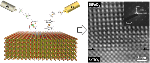
High-quality chemically complex
BiFeO3 oxide films on SrTiO3 substrate in
single-crystalline epitaxial form,
demonstrating applicability as an inexpensive,
easy, and highly scalable route ( From A. K.
Akbashev et al., Nano Lett. 14, 44 (2013)).
In the near future, the microelectronics industry will require materials solutions beyond CMOS with new and dramatically improved properties, providing innovative paradigms for information storage and data processing. Among possible candidates for this forthcoming revolution, oxides are very promising materials. They exhibit an exceptionally broad range of versatile functionalities (insulator to superconductor, ferroelectric, magnetic…) controllable by external stimuli (electric/magnetic fields, light, stress…) arising from the complex interplay between charge, orbital, spin and lattice degrees of freedom. The field of oxide electronics or “oxitronics” has consequently grown exponentially over the last 10 years. The advantages of this new “oxitronics” lie in: a) the exploitation of new functionalities exhibited by oxides, completely absent or weak in conventional semiconductors, b) their isostructure, which allows the vertical integration of multiple devices through epitaxial heterostructures, c) the striking possibility of size reduction thanks to their nanometric characteristic lengthscales. The impressive growth in the field of “oxitronics” has been achieved thanks to advances in film synthesis by pulsed laser deposition (PLD) or molecular beam epitaxy (MBE), but both techniques are hardly compatible with industrial processes. The next major step towards practical oxitronics would be to combine functional oxides with Si-CMOS technology. This would greatly extend the performance of silicon devices and even open the way to integrated circuits (ICs) built from functional oxides in order to fully exploit the functionality of oxides whilst maintaining the compatibility with current Si wafer production technology.
The main objective of AXION is to endow the Paris-Saclay campus with a dedicated tool allowing ALD (atomic layer deposition) processes facilities for the growth of large-area and high-quality oxide film on silicon wafers (2 inches). We will demonstrate our ability to design oxide-based devices with optimized properties as temperature sensors, ferroelectric tunnel junctions for new memories or future neuromorphic architectures, MEMS or GHz-THz electro-optical devices on Si. To achieve these objectives, the project brings together experts working on the physics of thin films and heterostructures of oxides, their modelling, their characterization and their use for potential innovative nanocomponents.
The AXION project will create or strengthen collaborations between the major actors of the Paris-Saclay oxitronic community. This will allow achieving a critical mass consortium working in a key area of condensed matter, strong and visible enough to develop new collaborations and respond to national and European projects. It will also favor interactions with industrials and foster the development of future joint projects. AXION also intends to strengthen links between research and education and plans to give lectures on growth of oxides and oxide-based devices at the International School and in masters.
Contact: , Unité Mixte de Physique CNRS/Thales
